Chapter 4 - Sequential Circuits

1 Sequential Circuit Definition
A circuit whose output depends not only on the present input but also on the history of the input is
called a sequential circuit.
Figure 4-1(a) is block diagram of a sequential circuit, formed by interconnecting a combinational circuit and storage elements. The storage elements are circuits that are capable of storing binary information. The binary information stored in
these elements at any given time defines the state of the sequential circuit at that time. The sequential circuit receives binary information from its environment via the inputs. These inputs, together with the present state of the storage elements, determine the binary value of the outputs.
The block diagram demonstrates that the outputs in a sequential circuit are a function not only of the inputs, but also of the present state of the storage elements. The next state of the storage elements is also a function of the inputs and the present state. Thus, a sequential circuit is specified by a time sequence of inputs, internal states, and outputs.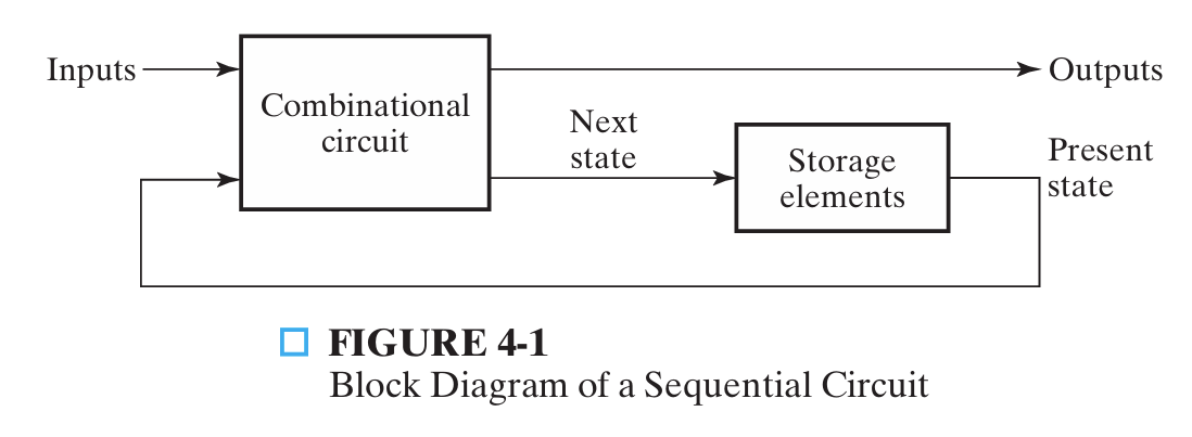
There are two main types of sequential circuits, and their classification depends on the times at which their inputs are observed and their internal state changes.
| 类型 | 核心定义 | 行为特征 |
|---|---|---|
| 同步时序电路(Synchronous) | 所有存储元件的时钟输入端连接到同一个全局时钟信号,状态更新严格同步发生在时钟的有效沿 | 行为由离散时间点的信号值定义,只有时钟脉冲到来时才会改变状态 |
| 异步时序电路(Asynchronous) | 没有统一的全局时钟,各个存储元件的时钟由前级电路的输出提供 | 行为由任意时刻的输入值和输入变化的顺序定义,状态逐个依次更新 |
同步时序电路的同步是通过时钟发生器(clock generator)这种时序器件产生周期性的时钟脉冲(clock pulse)序列来实现的。
同步存储元件只在每一个脉冲特定的时刻上受到影响
2 Latches
2.1 SR Latches
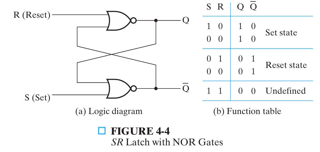
对于这个锁存器,我们来分析,
当S=R=0时,这时可以写出Q=Q,Q’=Q’,说明原先Q,Q’是什么,现在还是什么,不会变化
当S=1,R=0时,Q’一定是0,这时再看上面的或非门,0和0或非得到1,Q为1,此时Q和S异或得到0,我们说这个状态是稳定的
这时再把S=R=0,会发现Q=1,Q’=0,我们“记住”了这个结果
同理,把R=1,S=0,Q=0,Q’=1,接着把R设置回0,保存这个结果
不能做的是把S=R=1后又把S=R=0,因为S=R=1时,Q=Q’=0,这时又把S=R=0,Q和Q’都要变成1,这取决于谁先变成1,如果Q先变成1,Q’=0,反过来一样,所以我们无法确定Q和Q’是什么
使用与非门是同理的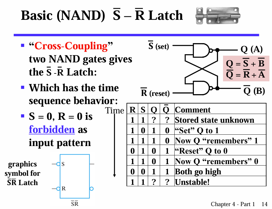
对于S’R’锁存器,同样地,如果先把S’=R’=0,那么Q和Q’就会先都是1,接着把S’=R’=1,如果门的延迟相同的话,Q和Q’然后同时变为0,又同时变为1……
这属于Unstable Latch Behaviors中的oscillation(振荡)
另一个不稳定行为是亚稳态,可以按下图理解,后面还会提及,Once you change an input, do not change it again until the circuit has had time to complete all its signal transitions and reach a stable state.
This is necessary to avoid the metastable behavior.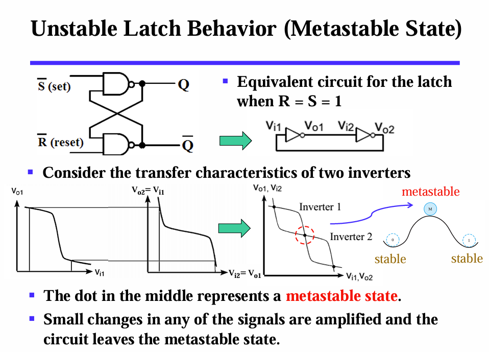
我们可以加上一个额外的输入控制信号,如果这个信号跟时钟脉冲序列有关,电路就变成同步的了,状态更新开始受时间控制,我们称指为SR触发器,虽然它并不是触发器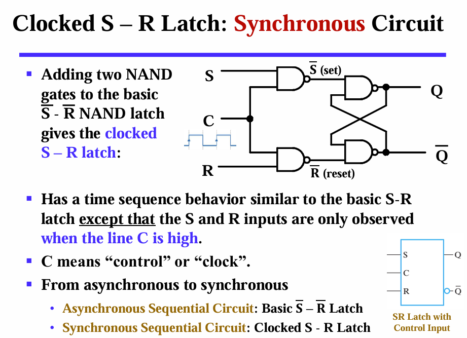
2.2 D Latches
既然不能出现S=R=1到S=R=0的情况,那么我们让S和R一定不一样就好了,但是要注意这也就不能“记住”一个状态了,因此我们使用D锁存器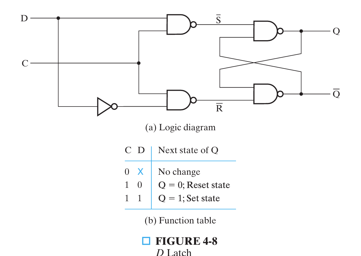
当控制信号为1时,Q的结果和D一样,而且Q和Q’的值一定相反,当控制信号为0时,无论D取什么,Q都不会变,即电路状态被记住,不会改变(其实就是S=R=0的情况),数据输入端在C从1变到0时的信息会一直保持在输出端Q不变,直到C再次变为1
3 Flip-Flops
As long as the pulse remains at the active (1) level,any changes in the data input will change the state of the latch. In this sense, the latch is transparent, since its input value can be seen from the outputs while the control input is 1.
例如我们把D锁存器的Q’接到D,那么只要C=1,假设初始Q为1,那么Q就会在0和1间反复横跳,最终状态取决于C=1的时长,这是我们不希望看到的
解决方法就是,在输出信号改变前,让输入信号与输出信号间的通路断开
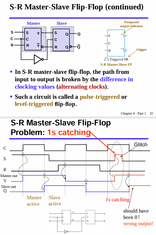
SR主从触发器,当C为1时,左边的锁存器(主锁存器)工作,右边的保持不变,当C变为0时,左边锁存器的结果作为右边锁存器的输入,右边锁存器输出左边锁存器在C=1时最后的结果,哪怕将Q’接到S,C=1时Y和Y’会一直跳,但Q保持不变
但是如果在C=1时,有一个glitch,S从0到1又变到0,那么主锁存器会记住S=1时Y=1的结果,这下C=0后Q就是1了,但本来没有glitch应该输出Q=0的,这就是1s catching问题
边沿式触发器(edge-triggered flip-flop)可以解决这种问题,它只在时钟转变的时候触发
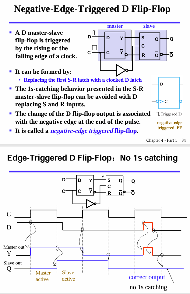
负边沿D触发器,当C=1时,Q保持不变,D是什么,Y就是什么,当C从C=1变到C=0时,第二个锁存器工作,Q=Y=D输出出来
当C=1时,D从0到1再到0是没问题的,因为Y相应地也会从0到1再到0,这就避免了1s catching问题
正边沿D触发器只需在C后面加一个非门即可
3.1 Direct Inputs
- At power up or at reset, all or part of a sequential circuit usually is initialized to a known state before it begins operation
- This initialization is often done outside of the clocked behavior of the circuit, i.e., asynchronously.
- Direct R and/or S inputs that control the state of the latches within the flip-flops are used for this initialization.

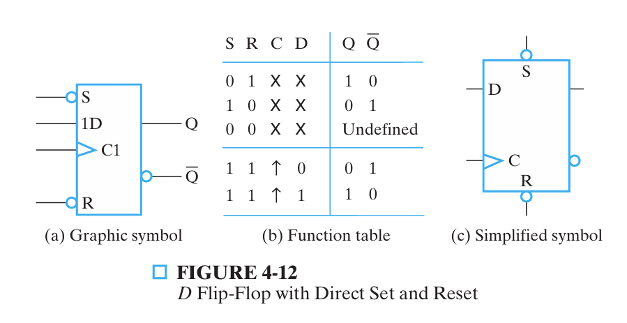
3.2 Symbols
第二行描述部分的符号,指正脉冲和负脉冲
第三行描述部分的符号指正边沿和负边沿
第三行C前的箭头表示C是动态输入,动态指示符号表示触发器在时钟脉冲的边沿跳变时才会响应
第二行的延时输出指示器符号表明输出信号在脉冲结尾才变化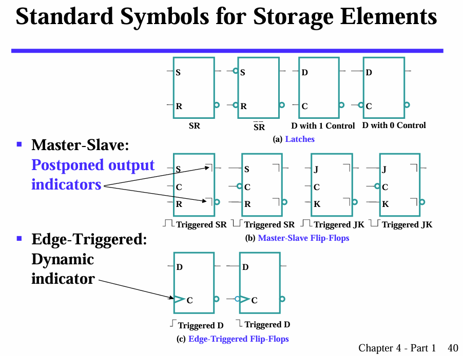
4 Flip-Flop Timing
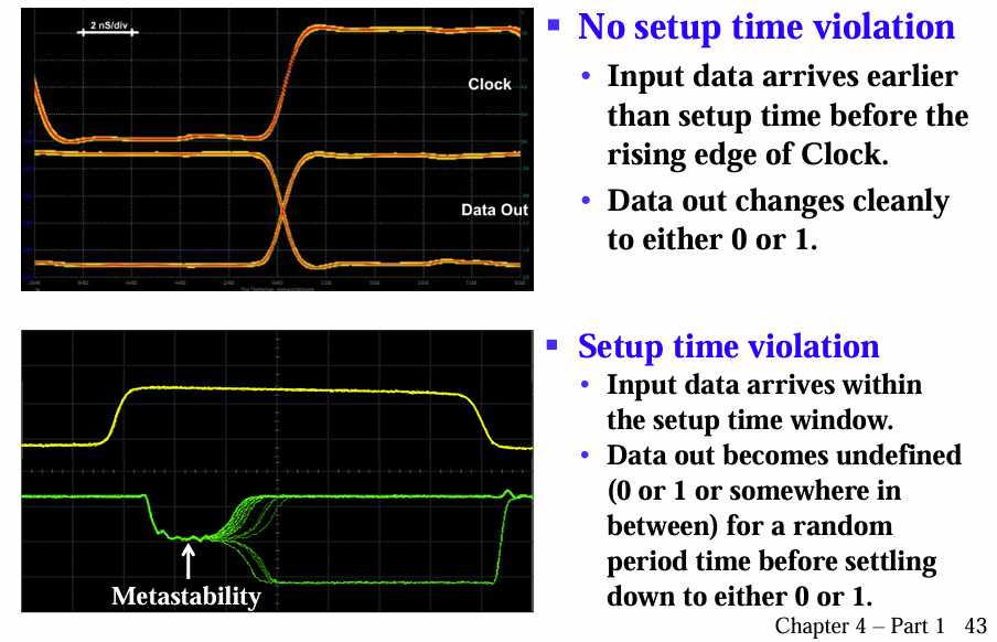
For both flip- flops, there is a minimum time called
the setup time,
Otherwise, the master could be changed erroneously in the case of the master – slave flip - flop or be at an intermediate(不确定的) value at the time the slave copies it in the case of the edge-triggered flip-flop.
Similarly, there is a minimum time called the hold time,
When a flip-flop samples an input that is changing during its aperture(也叫setup hold window,就是ts+th这段时间),the output Q may momentarily take on a voltage between 0 and VDD, that is in the forbidden zone. This is called a metastable state.
4.1 Flip-Flop Timing Parameters
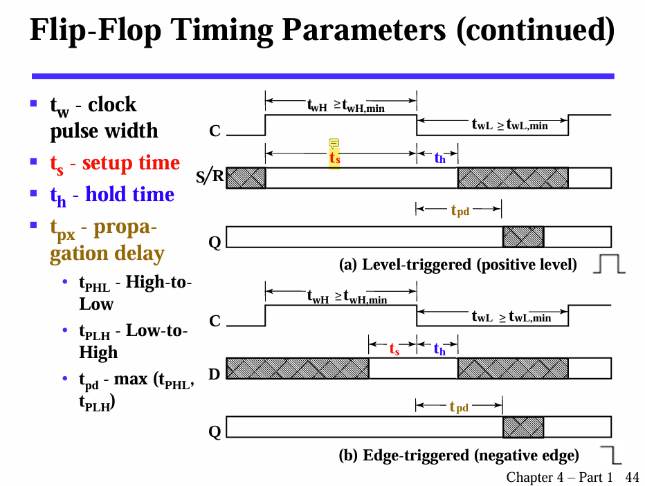
注意脉冲式触发器的set up time等于clock pulse width,因为这一段都必须保持稳定,这是为了避免1s catching问题,正如上面分析的,如果S变成1,哪怕立刻变回0(假设我们希望的输入是S=R=0),Y也会保持1,这时如果你仅保持C从1变到0前的一小段时间输入稳定,比如S=R=0,是错的
但D边沿触发器不一样,只要你在C从1变到0之前一小段时间保持D=1,结果就是1
此外要注意,ff的传播时间一般都长于且覆盖保持时间,一般认为
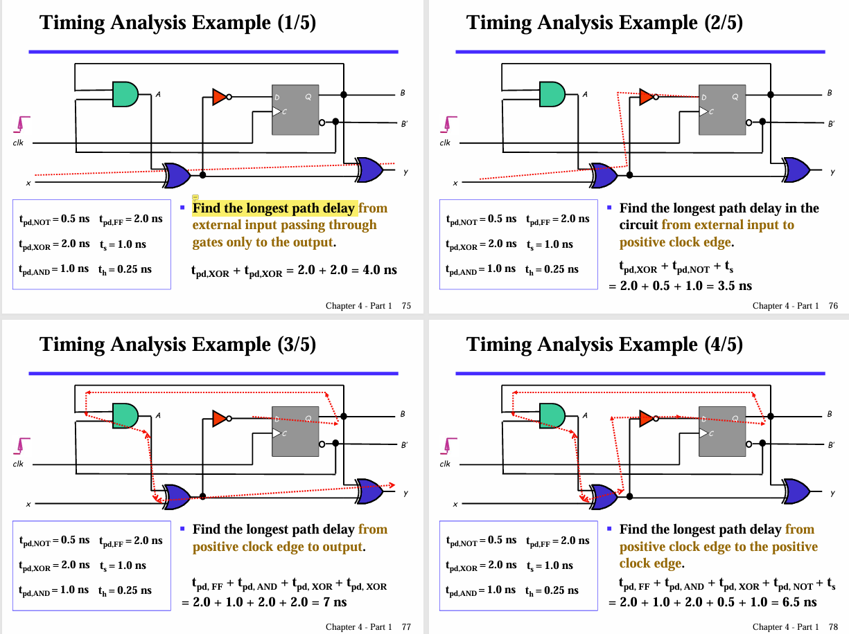
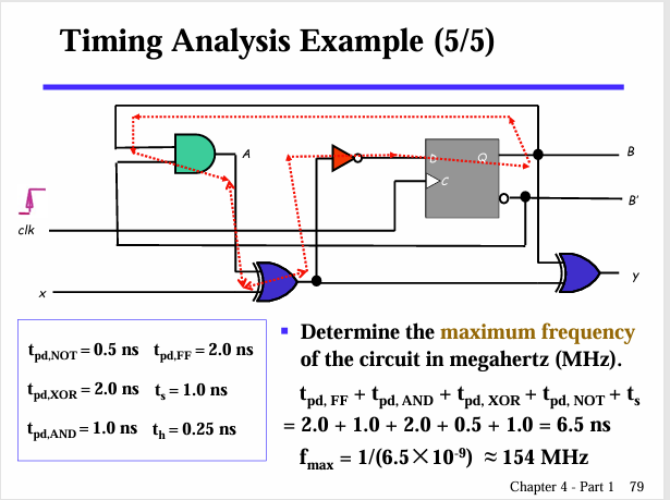
4.2 Timing Analysis of Sequential Circuits
关键是确认最大时钟频率,时钟频率等于时钟周期的倒数
时钟周期指两个触发边沿之间的时间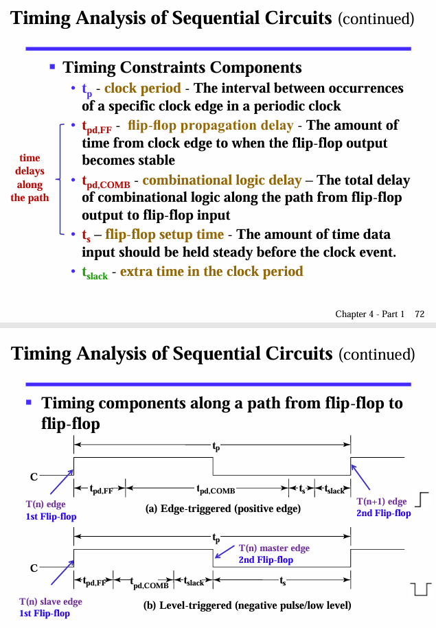
5 Sequential Circuit Analysis
- Identify the inputs, outputs, and internal states
- Determine the output equations, inputs and outputs of
flip-flops (i.e., input equations and next state equations) - Derive the state table (truth table with state):
• Inputs: inputs of circuit, present state of the circuit
• Outputs: outputs of circuit, next state of all flip-fops - List the next state of the sequential circuit
- Obtain a state diagram
- Analyze the performance of the circuit
- Verify the correctness of the circuit, check the self
recovery capability and draw the timing parameters
- Title: Chapter 4 - Sequential Circuits
- Author: Hare Fuyukawa
- Created at : 2026-05-17 11:32:55
- Updated at : 2026-06-03 17:38:49
- Link: https://redefine.ohevan.com/Logic-and-Computer-Design-Fundamentals/LCDF/LCDF-chapter4/
- License: This work is licensed under CC BY-NC-SA 4.0.