Verilog

Verilog Syntax
整数数值表示方法
数字声明时,合法的基数格式有 4 中,包括:十进制(‘d 或 ‘D),十六进制(‘h 或 ‘H),二进制(’b 或 ‘B),八进制(’o 或 ‘O)。数值可指明位宽,也可不指明位宽。
1 | // BINARY representations |
Numbers without a base_format specification are decimal numbers by default. Numbers without a size specification have a default number of bits depending on the type of simulator and machine (typically 32 bits)
1 | integer a = 5423; // No base format -> treated as decimal 5423 |
负数表示
通常在表示位宽的数字前面加一个减号来表示负数。例如:
1 | -6'd15 |
-15 在 5 位二进制中的形式为 5’b10001, 在 6 位二进制中的形式为 6’b11_0001。
Sections of Verilog Code
All behavior code should be described within the keywords module and endmodule. Rest of the design code would mostly follow the given template.
Verilog sections template
- Module definition and port list declaration
- List of input and output ports
- Declaration of other signals using allowed Verilog data types
- Design may depend on other Verilog modules and hence their instances are created by module instantiations
- The actual Verilog design for this module that describes its behavior
例如D触发器
1 | // "dff" is the name of this module |
Testbench Code
Testbench code
The testbench is the Verilog container module that allows us to drive the design with different inputs and monitor its outputs for expected behavior. In the example shown below, we have instantiated the flop design illustrated above and connected it with testbench signals denoted by tb_*. These testbench signals are then assigned certain values and are eventually driven as inputs to the design.
1 | module tb; |
Verilog Hello World
1 | // Single line comments start with double forward slash "//" |
A module called tb with no input-output ports act as the top module for the simulation. The initial block starts and executes the first statement at time 0 units. $display is a Verilog system task used to display a formatted string to the console and cannot be synthesized into hardware. Its primarily used to help with testbench and design debug. In this case, the text message displayed onto the screen is “Hello World !”.
Operator
1 | // Unary operator: operates on one operand |
Strings
1 | "Hello World!" // String with 12 characters -> requires 12 bytes (96 bits) |
Verilog Module
Syntax
A module is a block of Verilog code that implements a certain functionality. Modules can be embedded(嵌入) within other modules and a higher level module can communicate with its lower level modules using their input and output ports. They are the fundamental building blocks of digital hardware design, enabling modular, reusable, and hierarchical design methodologies
1 | // Basic module syntax with port list |
依旧D触发器的例子
1 | // Module called "dff" has 3 inputs and 1 output port |
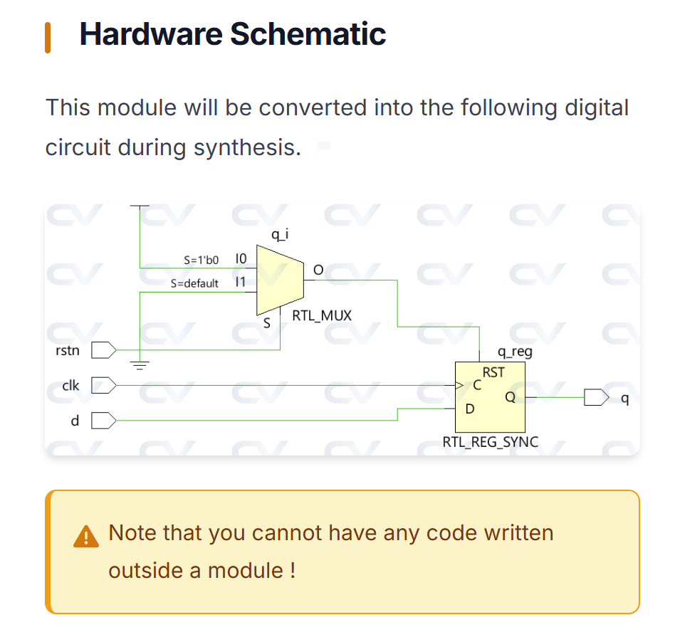
A module represents a design unit that implements certain behavioral characteristics and will get converted into a digital circuit during synthesis. Any combination of inputs can be given to the module and it will provide a corresponding output. This allows the same module to be reused to form bigger modules that implement more complex hardware.
例如,D触发器可以构成移位寄存器
1 | // 4-bit shift register built from four DFF module instances |
Top-Level Modules
A top-level module is one which contains all other modules. A top-level module is not instantiated within any other module.
Design Top Level
The design code shown below has a top-level module called design. This is because it contains all other sub-modules requried to make the design complete. The submodules can have more nested sub-modules like mod3 inside mod1 and mod4 inside mod2. Anyhow, all these are included into the top level module when mod1 and mod2 are instantiated. So this makes the design complete and is the top-level module for the design.
1 | //--------------------------------- |
Testbench Top Level
The testbench module contains stimulus to check functionality of the design and is primarily used for functional verification using simulation tools. Hence the design is instantiated and called d0 inside the testbench module. From a simulator perspective, testbench is the top level module.
1 | //----------------------------------------------------------- |
Hierarchical Name
A hierarchical structure is formed when modules can be instantiated inside one another, and hence the top level module is called the root. Since each lower module instantiation within a given module is required to have different identifier names, there will not be any ambiguity in accessing signals. A hierarchical name is constructed by a list of these identifiers separated by dots . for each level of the hierarchy. Any signal can be accessed within any module using the hierarchical path to that particular signal.
1 | // Hierarchical path examples using the design structure above |
Module definitions (the structural template) cannot be nested inside other modules. Verilog only supports module instantiation (creating instances of already-defined modules). Attempting to define a module inside another causes “illegal nested module definition” errors.
Best Practice: Define all modules separately at the top level of your file. Inside parent modules, only instantiate pre-defined modules: dff u0 (.d(data), .clk(clk), .q(output));
Verilog Ports
Ports are a set of signals that act as inputs and outputs to a particular module and are the primary way of communicating with it. Think of a module as a fabricated chip placed on a PCB and it becomes quite obvious that the only way to communicate with the chip is through its pins. Ports are like pins and are used by the design to send and receive signals from the outside world.
| Port Type | Description Use | Cases |
|---|---|---|
| input | The design module can only receive values from outside using its input ports | Clock signals, data inputs, control signals, reset |
| output | The design module can only send values to the outside using its output ports | Computed results, status flags, data outputs |
| inout | The design module can either send or receive values using its inout ports (bidirectional) | Memory data buses, I2C/SPI data lines, tri-state buses |
Ports are by default considered as nets of type wire. If you need an output port to be driven by a register (from an always block), you must explicitly declare it as output reg.
Syntax
1 | module my_design ( |
Each port must have a unique identifier within a module.
Signed Ports
Use signed ports when performing arithmetic that involves negative numbers, such as digital signal processing (DSP), coordinate calculations, or signed comparisons. For example, a 2’s complement signed 4-bit value can represent -8 to +7, while unsigned represents 0 to 15
If either the net/reg declaration or the port declaration has a signed attribute, then the signal shall be considered signed.
signed就意味着所有数都用补码形式表示
其中正数的补码就是原码,例如5的补码表示就是0101
用补码形式表示-5是1011
求法是正数表示取反+1(0101->1010, 1010+1=1011)
或者
Complete & Incomplete Declarations
If a port declaration includes a net or variable type (wire, reg), then that port is considered to be completely declared. It is illegal to redeclare the same port in a net or variable type declaration
1 | module test ( |
Verilog Module Instantiations
Bigger and complex designs are built by integrating multiple modules in a hierarchical manner. Modules can be instantiated within other modules and ports of these instances can be connected with other signals inside the parent module.
These port connections can be done via an ordered list or by name.
Syntax
One method of making the connection between the port expressions listed in a module instantiation with the signals inside the parent module is by the ordered list.
mydesign is a module instantiated with the name d0 in another module called tb_top. Ports are connected in a certain order which is determined by the position of that port in the port list of the module declaration. For example, b in the testbench is connected to yof the design simply because both are at the second position in the list of ports.
1 | module mydesign ( input x, y, z, // x is at position 1, y at 2, x at 3 and |
A better way to connect ports is by explicitly linking ports on both the sides using their port name.
The dot . indicates that the port name following the dot belongs to the design. The signal name to which the design port has to be connected is given next within parentheses ( ).
1 | module design_top; |
Unconnected/Floating Ports
Ports that are not connected to any wire in the instantiating module will have a value of high-impedance(阻抗).
1 | module shift_reg ( input d, |
仿真中,未连接的输入/输出端口会被赋予高阻态Z,综合后,未连接的输出会被悬空;未连接的输入可能会被接地(拉低)或保持高阻,取决于工具
All port declarations are implicitly declared as wire and hence the port direction is sufficient in that case. However output ports that need to store values should be declared as reg data type and can be used in a procedural block like always and initial only.
Ports of type input or inout cannot be declared as reg because they are being driven from outside continuously and should not store values, rather reflect the changes in the external signals as soon as possible. It is perfectly legal to connect two ports with varying vector sizes, but the one with lower vector size will prevail and the remaining bits of the other port with a higher width will be ignored.
1 | // Case #1 : Inputs are by default implicitly declared as type "wire" |
- Title: Verilog
- Author: Hare Fuyukawa
- Created at : 2026-05-25 15:24:31
- Updated at : 2026-06-03 17:38:49
- Link: https://redefine.ohevan.com/Logic-and-Computer-Design-Fundamentals/LCDF/LCDF-SP/
- License: This work is licensed under CC BY-NC-SA 4.0.